Why CNC Turned Brass Parts Fail in High-Performance Electronics — And the Design Decisions That Prevent It
Last quarter, I found a $40,000 shipment delay caused by one design decision made in the first week of a project. An RF connector housing had passed all dimensional inspections. Clean finish on the surface. Tolerances were in spec. But during system testing, signal loss was 23% above acceptable limits – and it took four days to find the root cause.
The engineer specified C360 free-cutting brass. It machines beautifully and quotes competitively. What C360 doesn’t have, versus the C260 cartridge brass, is the same level of conductivity consistency at high frequencies. That alloy choice was a manufacturability decision, not an electrical performance decision, and it resulted in micro-level resistance variation at RF signal levels that dimensional inspection can’t detect.
That’s the gap most design guides for brass electronics components never address. Here’s what actually matters.
Why Does Alloy Selection Matter More Than Most Engineers Realize?
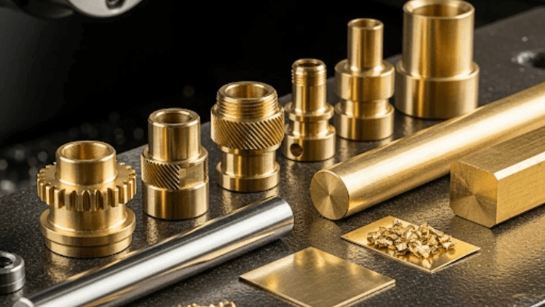
The brass family includes more than 40 different alloys with widely different electrical, mechanical,l and thermal properties. The single most common and most expensive mistake in the design of brass components for electronics is to treat them as interchangeable.
C360 (free-cutting brass, 61.5% copper) is machined at high speed with good chip control and low tool wear. It’s the default choice for most CNC turned brasswork and holes,tly the right choice for mechanical parts where electrical performance isn’t the main requirement.
C260 (cartridge brass, 70% copper) has higher copper content, better conductivity, a nd more predictable electrical behavior at high frequencies. It’s more difficult to machine – slower speeds, more tool wear, about 15-20% higher machining cost – but for RF connectors, precision contacts and high frequency shielding housings, the cost difference is trivial compared to the system-level performance risk of specifying the wrong alloy.
The decision tree is straightforward: if the part is to carry a signal or be a contact surface of precision, begin with electrical requirements and work backwards to alloy selection. Do not start with machinability and then expect the electrical performance to follow.
What Surface Finish Actually Does to Electrical Performance
The cosmetic finish of the surface of brass parts in electronics is not cosmetic. It has a direct influence on the contact resistance, repeatability of the transmission signal, and long-term corrosion behavior of the contact interface.
In the case of general connector housings and shielding components, standard CNC turning parameters can be used to achieve Ra of 0.816 -1, which is acceptable in most applications. In high-frequency connectors, performance variations can be measured in the range of Ra 0.4 µm or lower.
The number to know: The difference in insertion losses above 6 GHz can be measured when the surface roughness ranges between Ra 0.4 µm and Ra 1.6 µm on a precision RF contact surface. The difference is typically found in the noise of lower frequency. And then, to add to it, surface finish is not only an indicator of quality, but a signal-integrity variable.
A sharp and polished flute on the carbide tool cuts at a controlled rate and maintains a strict discipline in monitoring the tool condition during a production run. The supplier of an inconsistent tooling discipline will provide acceptable first articles and variable production runs. That is the trend to consider when screening suppliers and not when the first delivery is being made.
This is precisely why precision brass machining for electronics demands more rigorous process control than standard mechanical brass work — the performance consequences of surface variation are invisible to dimensional inspection but very visible in system-level testing.
How Plating Thickness Destroys Tolerances That Were Perfectly Designed
Here is the design error that causes the most expensive late-life rework in the electronics brass parts: imposing tight tolerances on features that will be plated, without considering the buildup of plating in the original design.
Contact reliability gold plating often imparts an additional 0.5 to 2.0 microns. Nickel undercoat 2-5 micron to provide resistance against corrosion. Solderability: Plating tin 2-10 microns (process dependent). A connector pin of 5-micron nickel + 2-micron gold stack, at 70 percent of your total tolerance budget, is a connector pin in which your component will be mounted.
The fix is 100 percent upstream design plated dimensions to the final plated size, not pre-plate machined size. Mark on the engineering drawing the ranges of plating thickness. And have an agreement with your machining supplier and plating supplier that they are operating to the same dimensional target. They are not typically unless a person says they are.
The Thermal Expansion Calculation Nobody Does Until It’s Too Late
Brass expands around 19 x 10⁻⁶ /°C. That is a dimensional change of about 0.025mm per 10mm of feature length across the entire temperature span of a connector housing between -40 °C and +85 °C – a typical industrial electronics temperature range.
This translates to 0.125mm thermal movement of a housing with a critical dimension of 50mm. Considering you have a tolerance of ±0.05mm in assembly, thermal expansion in itself will exceed your tolerance limit. This computation requires 3 minutes and can prevent a kind of field failure, which takes weeks to debug once installed.
Engineers working across demanding sectors of this industry — automotive electronics, aerospace instrumentation, industrial controls, telecommunications infrastructure — treat this calculation as a standard design step, not an afterthought. Account for differential expansion between the brass component and mating materials. Aluminum expands at 23 x 10⁻⁶/°C, stainless at 17 x 10⁻⁶/°C — different enough from brass to create assembly stress in temperature-cycling applications if clearances aren’t designed with movement in mind.
Thread Design and Micro Features: Where Small Mistakes Become Assembly Problems
Brass component threads look simple until they cause field failures. Most common issues: sharp internal corners leading to stress concentration at thread roots, poor control of thread depth causing weak engagement under vibration, and burr formation at thread exits impacting the assembly of the mating components.
The threads of brass components are not so easy as they lead to field failures. The most frequent problems include sharp internal corners that result in the localisation of stress in thread roots, inadequate control of thread depth that causes weak engagement during vibration, and the presence of burrs at thread exits that affect the assembly of the mating components.
Compared to cut threads, rolled threads possess superior fatigue characteristics and surface integrity in brass, and additionally, cold working of the thread material enhances the thread surface hardness at the thread form itself rather than leaving machined surfaces that can gall as the thread is assembled and disassembled. Lead chamfer Lead chamfers help to minimize the difficulty of forming burrs where thread entries occur. Dimensional sensitivity of the connection to manufacturing variation.n Dimensional sensitivity of the connection to manufacturing variation. Reducing the difficulty of forming burrs at the thread entry.s This is because at thread entries, the dimensional sensitivity of the connection to manufacturing variation is reduced by avoiding excessively fine thread pitches except where specifically required by the application.
The Pre-Design Checklist That Prevents Most Brass Electronics Failures
When making a final decision on any CNC turned part of brass to be used in an electronics application, be sure to check five things.
I am curious whether the alloy has been chosen due to electrical demands as opposed to machinability? Do the plated sizes have the final plated size and the ranges of thickness to be called out on the drawing? Has thermal expansion been calculated over the entire operating temperature range, taking into account differential expansion to mating materials? Has the surface finish been indicated by the Ra value of contact surfaces, rather than leaving it to the supplier’s default? Has the machining vendor attested to them controlling surface finish during manufacturing, and not only on the first parts?
In my experience, all the failures of electronics components in brass have contravened at least one of the following five points. The former, which is usually done during the first week of the project and before anyone has bothered, is known as the former.
What of these five are the most regularly omitted in your current design process when schedule pressure is high?
Popular on OTW Right Now!


About The Author
Gagan Bhangu
Founder of otechworld.com and managing editor. He is a tech geek, web-developer, and blogger. He holds a master's degree in computer applications and making money online since 2015.