
Why AI Hardware Needs Advanced PCB Design More Than Ever
Artificial intelligence is no longer confined to cloud servers or research laboratories. Today, AI powers everything from smartphones and laptops to autonomous vehicles, medical imaging systems, industrial robots, and smart home devices. The challenge for hardware companies is to provide more computing power in smaller, lighter, and more efficient devices as AI features become more ubiquitous in everyday gadgets.
These expectations cannot be met through the use of powerful computers or state-of-the-art software. Electronic devices must also change in order to be able to transmit data at a higher speed, perform better thermally, and become denser. It’s here that today’s printed circuit board (PCB) solutions are essential.
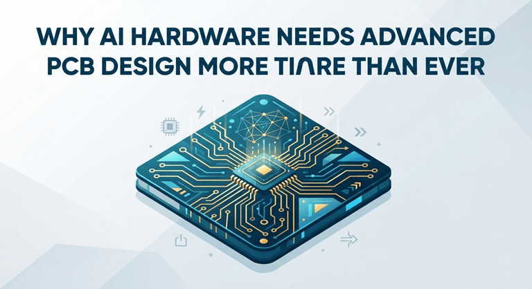
The Rise of AI Hardware Is Transforming Electronics Design
The technology of AI has transformed the design of electronic products, especially with its speedy adoption . With the swift adoption, the technology of AI has transformed the way electronic products are designed. AI-powered devices can also process vast quantities of data locally, which can lead to quicker decision-making, lower latency, and better privacy protection, unlike traditional consumer electronics that don’t have this feature. Edge AI is a growing trend in a variety of disciplines, such as healthcare, automotive, manufacturing, and consumer electronics.
According to the International Data Corporation (IDC), worldwide spending on AI technologies is projected to exceed $300 billion by 2026, driven largely by investments in AI infrastructure and intelligent devices. As AI workloads grow more complex, manufacturers have increasingly higher demands for more powerful processors, memory, sensors, and wireless communications devices in smaller hardware packages.
To achieve this balance between performance and size, many electronics companies partner with an experienced HDI PCB manufacturer capable of producing high-density interconnect boards that support advanced routing, faster signal transmission, and greater design flexibility. The growing adoption of AI technology has led to the integration of HDI technology as a key component in producing AI hardware. As AI technology continues to grow, HDI technology has become a crucial part of the development of AI hardware, especially in terms of space constraints.
Why Traditional PCB Designs Are No Longer Enough
While traditional PCB designs have been effective for the electronics industry for years, the electronics of today are presenting new PCB design challenges.
The lack of space is one of the greatest challenges. Engineers are challenged to fit intricate electrical routing into smaller devices such as thin laptops, sleek smartphones, lightweight wearable devices, and compact industrial equipment, all of which consumers are looking for. Different from traditional THR, this type of vias does not occupy board space and allows for greater component placement flexibility.
Signal integrity is also a growing concern. AI processors communicate vast amounts of data with memory and external components in a matter of nanoseconds. Bad PCB design may create signal degradation, electromagnetic interference (EMI), mismatches in impedance, and crosstalk, which all have the effect of compromising system stability and performance.
Thermal management is also a challenge. AI accelerators and high-performance processors generate a lot of heat when in use. If not carefully designed and optimized with power distribution, the excessive temperature can cause the components to have a shorter lifespan and decrease the reliability of the device.
With the complexity of hardware increasing, manufacturers are also introducing multi-layer PCB structures, fine-pitch ball grid array (BGA) packages, and advanced semiconductor packaging technologies that are beyond the capabilities of traditional PCB manufacturing processes.
How HDI PCB Technology Solves Modern AI Hardware Challenges
The technology of High-Density Interconnect (HDI) PCB was created to meet the escalating complexity of electronic products. HDI boards make use of laser-drilled microvias, blind and buried vias, and ultra-fine trace widths, which not only add to the density of routing but also decrease the overall size of the board.
The benefit of HDI technology is that it allows more components in a given space. Engineers can also reduce the length of electrical paths, maximize the efficiency of routing, and better make use of layers without increasing the physical size of the device.
Signal integrity is another factor that is improved by HDI designs. Unlike longer traces, the shorter length will cause less loss of signal, and better impedance control will reduce the amount of reflection and interference. These properties are especially crucial for AI processors, high-speed memory interfaces, PCIe communication and next-generation wireless technologies like Wi-Fi 7 and 5G.
Thermal performance is also enhanced. Placing components in better locations aids in the distribution of heat-generating devices, enhances cooling opportunities, and promotes better air flow. When paired with optimized power delivery networks, HDI PCBs help ensure a consistent performance level during heavy AI workloads.
The benefits of HDI technology are why it has taken over in numerous high-performance electronic products.
Why Choosing the Right PCB Manufacturing Partner Matters
Creating an HDI PCB design is just one component of the process. Manufacturing accuracy, engineering skill, and quality control are essential to a successful production.
An experienced PCB manufacturer can offer product development support at every stage by providing Design for Manufacturability (DFM) analysis, stack-up optimization, material selection suggestions, and production feasibility analysis. By working together from the outset, problems can be spotted early and so prevent significant production delays.
It’s also important to consider manufacturing capabilities. The laser drilling equipment must be able to punch very small microvias, multilayered structure lamination processes must be advanced, and the automated optical inspection (AOI) and X-ray inspection for the hidden solder joints are required. In addition, it is necessary to strictly control the process throughout the manufacturing process.
Quality assurance should never be forgotten. Reliable manufacturers usually meet international standards like quality management systems based on ISO, electrical performance, and mechanical reliability, which are usually tested as per IPC specification, etc. The quality practices are particularly significant in industries where hardware failures may have significant consequences, such as in automotive electronics, medical devices, and industrial automation.
Industries Already Benefiting from HDI PCB Technology
The impact of HDI PCB technology extends far beyond consumer electronics. Numerous industries now rely on high-density circuit boards to support increasingly sophisticated AI applications.
AI PCs and High-Performance Laptops
The newest iteration ofAI-poweredd PCs comes with its own dedicated neural processing unit (NPU) alongside high-powered CPUs and GPUs. The added components for processing need very optimized motherboard designs, which can achieve very fast processing speeds in small sizes. These complicated designs are possible due to HDI PCBs.
Smartphones and Wearable Devices
The combination of AI image processing, advanced camera systems, biometric sensors, multiple wireless antennas, and more powerful chipsets packed into the ever-thinner smartphones is a fascinating mix. Even tighter space constraints are imposed on smartwatches and fitness trackers. The manufacturers can use HDI technology to pack maximum functionality in a device while keeping its size minimal.
Automotive Electronics
High-speed electronic communication is vital for Advanced Driver Assistance Systems (ADAS), intelligent cockpit systems, electric vehicle control units, and autonomous driving platforms. HDI PCBs are used to increase the stability of the signal and to meet the tough environmental criteria for automotive use.
Medical Devices
In the fields of portable ultrasound technology, patient monitoring, wearable health monitoring devices, and AI-driven diagnostic tools, compact and reliable electronics are needed to power technology that must be capable of functioning continuously with unmatched precision. These mission-critical technologies in healthcare require precision and reliability, which are provided by HDI boards.
Industrial Automation and Robotics
As the Internet of Things (IoT) becomes more pervasive, factories are increasingly adopting the use of AI-driven machine vision systems, autonomous mobile robots, predictive maintenance platforms, and edge computing devices. Such industrial systems demand rugged electronic assemblies that will reliably function for long periods and perform complex processing.
Emerging Trends Shaping the Future of AI PCB Design
With the continuing evolution of AI technology, PCB design requirements will become tougher and tougher.
Edge computing is one of the significant trends that is booming. More AI processing will take place on local devices, instead of sending all the data to cloud servers. This transition demands more and more advanced embedded hardware with advanced PCB architectures.
High-end semiconductor packaging solutions such as chiplets and System-in-Package (SiP) designs are also gaining popularity. These innovations allow a higher level of integration in a denser layout, while requiring more precision in PCB manufacturing.
Sustainability is also a growing concern. To minimize the impact on the environment during the lifetime of the product, electronics manufacturers are looking for recycling opportunities and developing more energy-efficient production processes and environmentally friendly lamination materials.
Going forward, greater miniaturisation, enhanced automation, and smarter design optimisation will be essential to fulfill the needs of the next generation of applications for AI.
Key Considerations When Selecting an HDI PCB Partner
The decision on who to partner with for manufacturing should not be a simple price comparison. When choosing to build an AI hardware startup, there are a number of factors that need to be taken into account, such as engineering skills, the ability to prototype, scalability of production, quality certifications, inspection technology, supply chain stability, and technical support.
Manufacturers with proven experience in complex multilayer HDI fabrication often have more resources to meet the changing demands of products and to shorten time to market. Effective communication during the design can also minimize revisions, yield improvement, and reduce the cost of manufacturing.
Conclusion
From consumer electronics to industrial infrastructure, AI is poised to revolutionize almost every type of electronic gadget or device. With the growing power of computers and miniaturisation of electronic devices, the use of traditional PCB technologies in modern product design is proving to be unsuitable.
HDI PCB technology offers the routing density, signal integrity, thermal characteristics, and reliability essential to enable the innovations of today’s AI. From smart medical devices to self-driving cars, from AI-PC to intelligent manufacturing systems, the key to high-tech product design is not just a part of the manufacturing process—it’s a strategic asset.
High-quality HDI solutions combined with a knowledgeable manufacturing partner will enable companies to develop faster, smaller, and more reliable AI products and stay competitive in a tech-driven world.
Popular on OTW Right Now!



About The Author

Gagan Bhangu
Founder of otechworld.com and managing editor. He is a tech geek, web-developer, and blogger. He holds a master's degree in computer applications and making money online since 2015.