
Photochemical Etching for AI Hardware
AI hardware is often discussed in terms of processors, memory, software models, and advanced PCB design. Yet reliable performance also depends on the small physical parts surrounding these systems. Shielding covers, contacts, fine screens, spacers, and sensor parts help manage interference, alignment, airflow, and signal flow. For teams developing compact systems, photochemical etching offers a practical way to produce thin, detailed metal parts without the cutting forces used in conventional machining.
Why AI Hardware Places More Pressure on Physical Components
AI-powered devices can handle more data, transmit data at quicker speeds, and are often smaller in size. All of the components of the hardware stack are under pressure due to these conditions. High-speed circuits may be more susceptible to electromagnetic interference. Larger crowding results in less”“safe spac””, connectors, and thermal structures. The size of the device may also demand smaller aperture and spacing between components.
Edge devices, robotics, medical devices, smart cameras, industrial sensors, and consumer electronics are all impacted by these challenges. A seemingly insignificant metal component can be a significant problem if it is not fitted properly, has an unwanted burr, or is not sufficiently geometrically consistent, since these factors can negatively impact assembly and reliability.
The Components Working Around the PCB
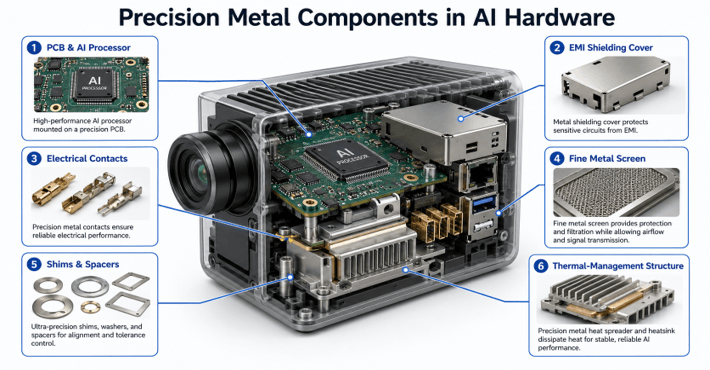
The PCB is the core of an electronic system, butit’ss not the only one to perform. The board and greater device could have several thin metal components supporting them.
EMI and RFI shields are used to isolate sensitive circuits or contain noise from high-speed circuits. Electrical contacts and lead frames are used for passing both signals and power. The fine metal screens can function as airflow, filtration, or protection.
Alignment control and controlled gaps are achieved with shims and spacers. Encoder disks and sensor plates provide motion and feedback functions.
While these components have unique functions, they all have similar manufacturing needs – thin material, very small holes, clean edges, and repeatable dimensions.
How Photochemical Etching Produces Detailed Metal Parts
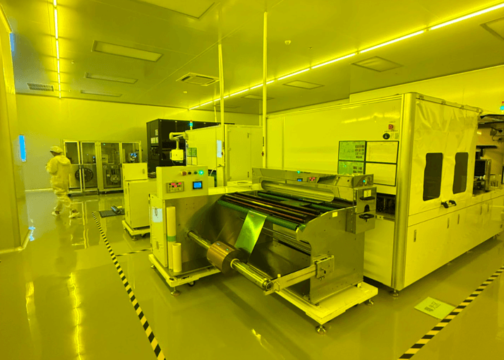
Photochemical etching (also known as photo etching or photochemical machining) is a metal sheeting process that uses a chemical process to remove areas from a metal sheet selectively.
A light-sensitive photoresist is applied to the sheet. UV exposure is used to transfer a digital pattern. Once developed, specific areas are protected, and an etchant dissolves the exposed metal. Thereafter, parts are stripped, cleaned,d and inspected.
The process does not require mechanical pressure on the part, avoiding direct mechanical pressure on the piece. It can perforate, slot, grid, tab, mark, and print half-etch bend lines in a single flat pattern.
It is also easier to make changes to digital artwork. With engineers making changes to a feature or running multiple versions, there is no need to make a new hard die for each change.
Why Etching Fits High-Density Electronics
The parts for high-density electronics frequently have numerous small features. Multiple operations can be needed to form multiple openings or profiles using mechanical methods, but photochemical etching can perform them simultaneously.
It could also be applied to thin metals that are sensitive to force or heat. It can create parts without the raised burrs typically found when a part is manufactured by mechanical blanking. This can help minimize finishing work and minimize sharp edges that can impact assembly.
Material choices range from stainless steel, copper alloys, and nickel alloys to other metals chosen for their conductivity, corrosion resistance, strength, and/or formability.
For developers of lead frames, the ability to combine ventilation holes, mounting tabs, contact points, identification marks, and bend lines in one blank can simplify design and manufacturing.
EMI Shielding in AI Systems
AI hardware frequently integrates high-speed processors, wireless connectivity, power electronic components, and compact signal connectivity. The systems can produce or be affected by electromagnetic noise.
Board-level shielding helps to shield or enclose sensitive areas or to contain interference at its origin. They are affected not only by the metal itself but also by its performance. All gaps, seams, contact areas, grounding, vent patterns, and material choice are important.
Complex outlines and small perforations can be included in a photo-etched shielding part, and it is still thin and lightweight. Folded half-etched lines could also aid the subsequent forming into covers or frames.
The same technique can be used for edge AI, robotics, communications devices, medical electronics and industrial controls.
Other Metal Parts That Support Reliability
Shielding is just one such example. Etched lead frames, contacts, springs, screens, shims, spacers, apertures,s and encoder components are all potential components of AI hardware.
Electric lead frames and contacts provide electrical connections; screens can be used to protect openings and/or direct the flow of air. Shims and spacers control the height and alignment of assemblies. Motion/position feedback is provided by encoder/sensor parts.
Etched plates, screens, or fine structures can be used to support the airflow, spacing, or fluid distribution in thermal-management assemblies. These components can not independently address thermal issues; however, they can be part of a larger thermal-management system.
When Engineers Should Consider Photo-Etched Parts
Photochemical etching is worth considering when a part:
- Uses thin metal sheet or foil.
- Contains many holes, slots, or repeated patterns.
- Requires clean edges and low mechanical stress.
- May need several design revisions.
- Includes tabs, fold lines, or identification features.
- Must move from prototype to repeat production without major tooling changes.
It is not suitable for every component. Three-dimensional thick parts might be more appropriate for CNC machining. Stamping tools may be justified for simple parts that are made in very high quantities. There may be occasions when a thicker flat part is more cost-effective to laser cut.
That same process-fit logic applies to the connective hardware around the board. Etching suits thin, flat features, but the load-bearing contacts that actually mate and carry current are machined — precision-turned connector pins held to micron tolerances so they keep a stable, low-resistance grip as AI hardware shrinks and runs hotter.
Geometry, material, tolerance, thickness, production volume, forming requirement, finishing, and total project cost should be taken into consideration for the final decision.
Beyond Chips and Software
The success of reliable AI hardware is more than just processors and PCB designs. It also relies on the physical elements that protect, connect, align, clean, and support the system.
Professional metal etching gives engineers another option for creating fine features in thin metal. Its value is strongest when product teams need detailed geometry, clean edges, flexible design changes, and a practical path from prototype to production.
As AI hardware technology shrinks and becomes more powerful, such small parts will be even more critical in ensuring the overall reliability of the system.
Popular on OTW Right Now!




About The Author

Gagan Bhangu
Founder of otechworld.com and managing editor. He is a tech geek, web-developer, and blogger. He holds a master's degree in computer applications and making money online since 2015.